Insights
・
.
.
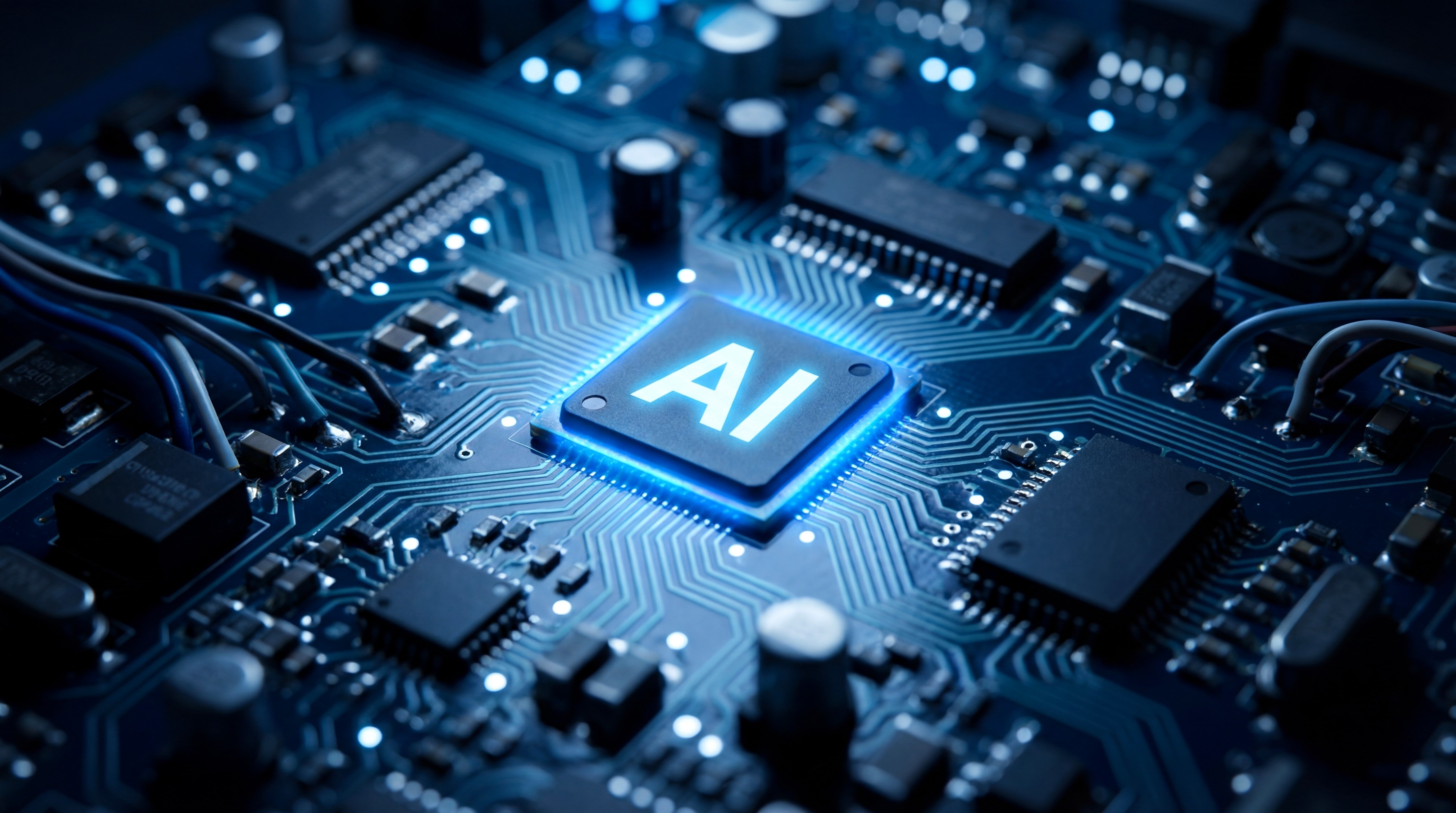
AI PCB design automation trends: What's actually changing in 2025–2026
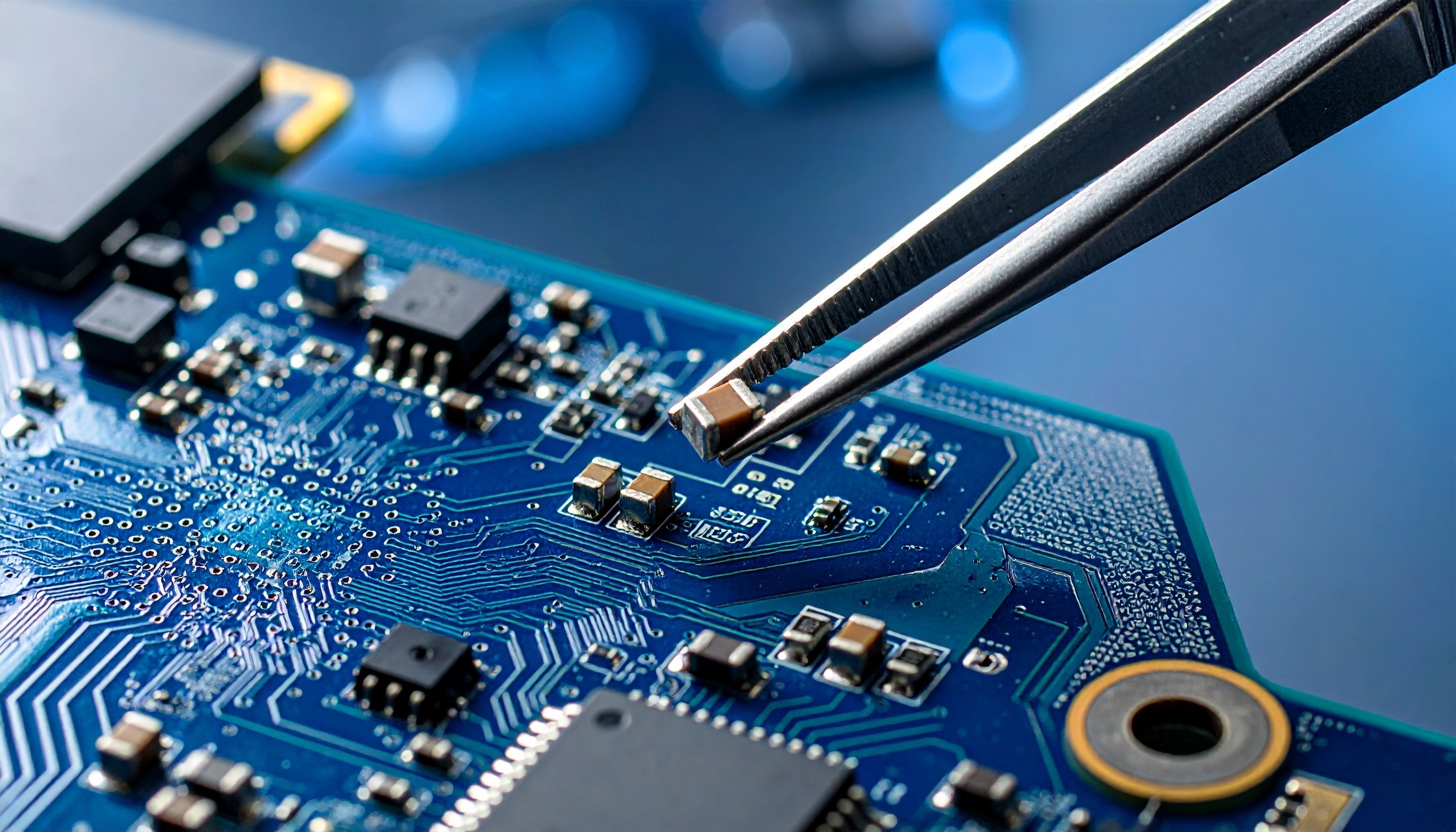
PCB layout has long been a bottleneck in hardware development. AI is finally breaking that logjam — starting with the two tasks engineers dread most: placement and routing.
💡 At a glance
Browser-based AI tools are making professional-grade design automation accessible without expensive software licenses or complex installations.
AI can now generate viable initial results for placement and routing — the most labor-intensive stages of PCB layout — cutting turnaround time significantly.
The bigger shift is explainability. Leading tools aren't just delivering outputs anymore. They're surfacing the reasoning behind each design decision, giving engineers something they can actually audit and trust.
If you've spent any time doing PCB layout by hand, you've probably had this thought: "There has to be a better way to handle all this repetitive work."
For EE students grinding through component placement for the first time, or junior engineers staring down a tight deadline with a 100-part schematic, that frustration is familiar. And heading into 2025–2026, the tools are finally starting to catch up.
1. Why PCB design automation is having its moment
The push to automate PCB design has been around for years. What changed is that around 2024–2025, three things finally converged — and the pace of development has been noticeably different since.
AI reached a point where it's actually useful. Models trained on large PCB design datasets can now produce placement and routing results that genuinely account for physical constraints and design rules. For standard embedded and IoT designs, that means simultaneously factoring in signal flow, thermal management, and design-for-manufacturability — in a single pass. That kind of multi-variable reasoning would have been a stretch to claim just a few years ago.
Getting started stopped requiring a setup process. AI computation runs server-side; the engineer just needs a browser. No installation, no license key, no week-long onboarding. For students and early-career engineers especially, that's not a small thing — it's the difference between trying a tool and not trying it.
The pressure to move faster isn't going away. As PCB-dependent products multiply across IoT, wearables, and mobility, design workloads have scaled with them. Faster time-to-production has shifted from a competitive advantage to a baseline expectation. AI automation is increasingly part of how engineering teams meet that bar.
2. What AI can actually do: placement and routing
The two areas where AI delivers the most practical value in PCB design today are component placement and routing.
With placement, the engineer uploads a schematic and the AI determines optimal component positions based on physical principles and established design rules — applying the same spatial reasoning that experienced engineers develop over years of hands-on work.
What separates the better tools is that they don't just hand you a result and move on. They surface the reasoning behind each placement decision, so you can review the output critically, push back where something looks off, and make an informed call. That's a meaningful difference from a black-box output you're expected to just trust.
With routing, the engineer uploads a completed placement file and the AI connects components while enforcing design rules throughout. Built-in real-time DRC catches violations as they occur — which tends to surface more issues than a manual review pass after the fact, and catches them earlier.
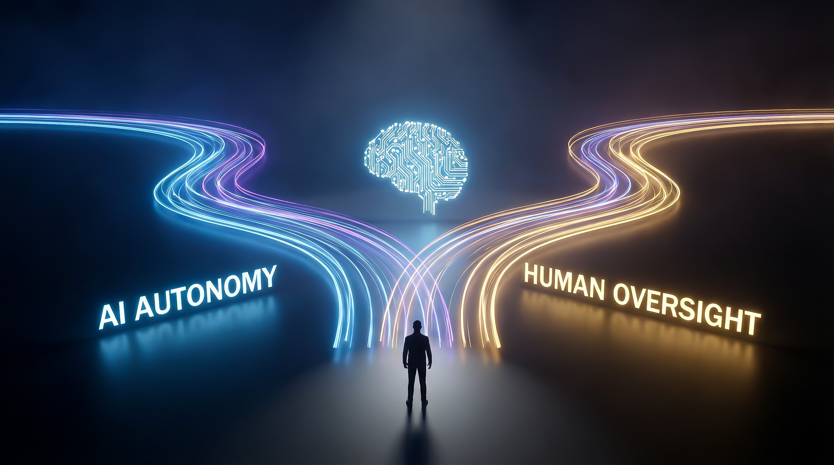
3. Where AI still has limits — and why that's worth knowing
AI handles a meaningful share of placement and routing work. It doesn't handle everything, and it's worth being clear-eyed about where the gaps are.
High-speed signal integrity work requiring tight impedance control, thermal analysis for high-power designs, manufacturer-specific fabrication constraints, and post-layout noise troubleshooting are still firmly in the engineer's domain. AI is strong at executing well-defined, repeatable tasks quickly and consistently. Anything requiring contextual judgment, domain intuition, or experience-based tradeoffs still needs a human in the loop.
The right framing isn't "AI replaces the engineer." It's closer to: AI takes the repetitive execution off your plate so you can focus on the work that actually requires your judgment.

4. How the EDA tool market is responding
If AI has real limitations, why is the market moving so aggressively in this direction? Because the tools are evolving specifically to close those gaps — and two shifts stand out.
The first is accessibility. Free and low-cost subscription tools that run entirely in the browser are quickly becoming the default entry point. The upfront cost and friction that previously kept students and smaller teams on the sidelines is largely gone.
The second is a push toward explainability. AI outputs only get used in real workflows when engineers can understand and trust the reasoning behind them. Tools that show why a component ended up where it did — not just where it landed — are gaining ground. Not every tool is there yet, but the direction the industry is moving is clear.