Insights
・
.
.
JLCPCB ordering guide: from gerber export to essential specs and customs tips
Whether you're building a custom keyboard, an Arduino project, or an IoT device, there’s a common hurdle every maker eventually faces: PCB fabrication.
💡 At a glance
Easily generate Gerber files with just a few clicks using MODI Factory's AI-driven auto-placement and routing features.
Discover clear guidelines for navigating complex JLCPCB manufacturing options, such as surface finishes and removing board marks.
Learn essential international shipping and customs tips, including cost-effective delivery choices, the $150 tax exemption limit, and PCCC requirements.
✅ Recommended for:
Anyone looking to save time on complex PCB routing and Gerber generation to focus on core circuit ideas.
Students and junior makers ordering from JLCPCB for the first time who feel overwhelmed by unfamiliar manufacturing options.
Buyers seeking a clear guide to international shipping and customs to avoid unexpected taxes or delivery delays.
Whether you're building a custom keyboard, an Arduino project, or an IoT device, there’s a common hurdle every maker eventually faces: PCB fabrication.
As a global PCB manufacturing service, JLCPCB is one of the most popular platforms among makers worldwide thanks to its cost-effectiveness and fast turnaround times. However, you’ve probably experienced the frustration of finishing your board design, confidently navigating to the order page, and then closing the tab in a panic when confronted with dozens of obscure options and complex jargon.
Today, we’ll walk you through the entire process—from preparing Gerber files using MODI Factory to selecting the right order options and navigating shipping and customs—so even beginners can get it right the first time.
1. Extracting JLCPCB-Ready gerbers in 3 Steps with MODI Factory
You no longer need to spend hours on manual component placement and routing. With MODI Factory, you can easily generate Gerber files tailored to JLCPCB's specifications.
① AI auto-placement and auto-routing
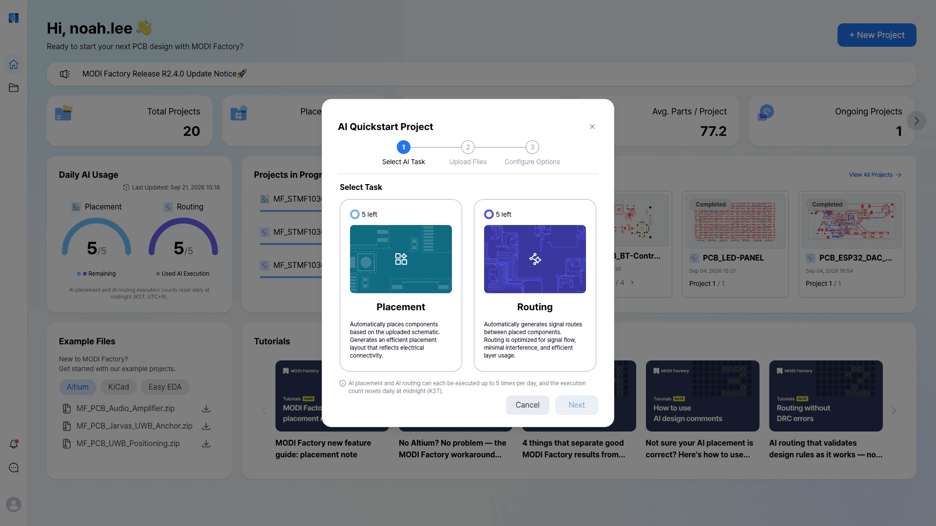
Once your schematic and layout files are ready, you can run the auto-placement and auto-routing features directly in MODI Factory.
Placement notes: Provides clear reasoning for component positioning, such as "why decoupling capacitors are placed at this specific distance from a certain IC" or "why noise-sensitive components are isolated in a specific zone."
Routing notes: Explains why traces were routed through specific layers to ensure signal integrity (SI) and validates the use of vias and routing paths, giving you full confidence in the generated layout.
② Inspect the engineering rationale via placement and routing notes:

MODI Factory does not operate as an opaque black box. You can open the dedicated notes to verify the design logic:
Placement notes: Outlines why specific bypass capacitors are placed within strict proximity to an IC, or why noise-sensitive analog components are isolated to specific zones.
Routing notes: Explains layer transitions, via allocations, and return paths chosen to maintain signal integrity (SI).
③ Export gerber files

Once you’ve finalized the placement and routing, extraction takes just a few clicks.
Click the hamburger menu (≡) on the top menu bar.
Select [Generate Gerber files] from the dropdown list.
Choose your desired format and download the ZIP file.
2. The ultimate guide to JLCPCB uploads and quote options

Drag and drop the Gerber ZIP file exported from MODI Factory into the [Add gerber file] section at the top of the JLCPCB Instant quote page. The dimensions and layer count will be automatically detected, and the options panel will appear.
① Default options you can safely leave as-is
The default settings represent the global industry standard and offer the most reliable, cost-effective combination. Unless you have specific requirements, leave them untouched.
Base material & PCB Thickness (FR-4 / 1.6mm): This is the undisputed industry standard worldwide. It offers the best balance of durability, manufacturability, and price.
(Note) Special materials like aluminum, Rogers (for high-frequency designs), or flexible boards, as well as thicknesses under 0.8mm, will drastically increase the cost. Stick to FR-4 and 1.6mm unless absolutely necessary.Outer copper weight (1oz): This standard thickness comfortably covers general signal traces and low-power circuits. Unless you're designing a high-current power supply board, 1oz is plenty.
Via covering (Tented - Default): This covers the via holes with soldermask ink. It prevents unwanted solder bridges (shorts) during manual hand-soldering, so it's highly recommended to keep this default.
Board outline tolerance (±0.2mm - Regular): Keep the default.
② Options you must check based on your project
These settings directly affect your board's finish, soldering difficulty, and visual appearance, so review them carefully.
(1) Surface finish
This is the coating applied to exposed copper pads to prevent oxidation.
HASL (with lead) / Lead-free HASL: The most affordable option, perfectly fine for through-hole (DIP) components or standard hobbyist circuits. However, the pad surface can be slightly uneven.
ENIG (Electroless nickel immersion gold): Provides a perfectly flat surface, which is essential for soldering fine-pitch ICs, QFN, and BGA components. It is highly resistant to oxidation and gives a premium gold aesthetic.
OSP: A thin organic coating that is cheap but has a short shelf life and poorer reworkability.
Tip: Choose HASL (Lead-free recommended) for simple hobby circuits. For soldering fine-pitch components or achieving a commercial-grade look, go with ENIG.
(2) Remove mark
JLCPCB automatically prints an internal production serial number (e.g., a string starting with JLC...) on an empty silkscreen area of your board.
If left as-is: It doesn't affect functionality, but it might print over your top artwork or text, ruining the aesthetics of a display board or finished product.
How to fix it: Check the [Remove mark] option (incurs a small extra fee). If the board will be visible outside of an enclosure, or if you want a pristine silkscreen on the front, you should definitely select this option.
3. Payment, Shipping, and customs clearance tips
Once you've configured your board options and added the order to your cart, the final hurdles are payment and international shipping.
① Choosing a shipping option
JLCPCB offers a variety of global shipping methods. Choose the one that best fits your project's urgency, budget, and the order's size/weight constraints.
Note before shipping: Shipping carriers, freight costs, and estimated delivery times vary greatly depending on the destination country and the parcel's weight and volume. The table below is an example based on South Korea. Before checking out, make sure the Country/Region is correctly set in your cart.
Carrier | Typical transit time | Best use case |
|---|---|---|
UPS Worldwide Express Saver | 2–5 business days | Optimal balance of speed, reliable tracking, and competitive pricing for small batches. |
FedEx Express | 3–6 business days | Reliable express courier service with global coverage. |
DHL Express | 1–3 business days | Fastest transit window; best for critical prototyping deadlines where delivery speed is the priority. |
S.F. Express Economy | 5–7 business days | Balanced regional courier option with moderate transit times. |
Postal service (e.g., E-POST) | 10–16 business days | Lowest shipping cost, but strictly restricted to small orders (typically under 1.5 kg, values under $150, and smaller parcels). |
Selection tip: For South Korea, the cheapest option, E-post ($6.58), takes 10–16 days and has strict size restrictions. For just about $3 more, you can use Ups Worldwide Express Saver ($9.49) and receive your boards in 2–5 days, making it the most practical choice. (For large-scale production orders over 100kg, sea freight is also an option.)
② Overseas customs clearance precautions
Personal Customs Clearance Code (PCCC) required: You must enter your 13-digit code starting with 'P', issued by the Korea Customs Service Uni-pass, in the recipient information on the order form.
Caution: The recipient's real name entered during checkout must exactly match the name registered to the PCCC to avoid customs holds.Duty-free limit ($150): Direct shipments from China are exempt from tariffs (list clearance/small-value exemption) if the combined value of the goods and local shipping is under $150 USD. Most simple sample boards fall within this limit. However, if you have a bulk order or include SMT assembly (component placement) that pushes the total over $150, you may be charged customs duties and VAT (around 10%). (Note: E-post cannot be selected for orders exceeding $150.)
Entering your address in English: To prevent delivery mishaps, use a local portal site's 'English address converter' to input your road name address and 5-digit zip code accurately.