Insights
・
.
.
How to choose the right PCB layer count for your project
Understand cross-sectional stack-up structures and key characteristics to choose the optimal PCB layer count for your project.
💡 At a glance
A cost-effective 2-layer board is ideal for simple control circuits, while a 4-layer board is highly recommended for stability in designs involving wireless communication or high-speed interfaces.
Forcing a complex design onto a 2-layer board just to save manufacturing costs often leads to EMI noise issues and inevitable respins, ultimately wasting more time and budget.
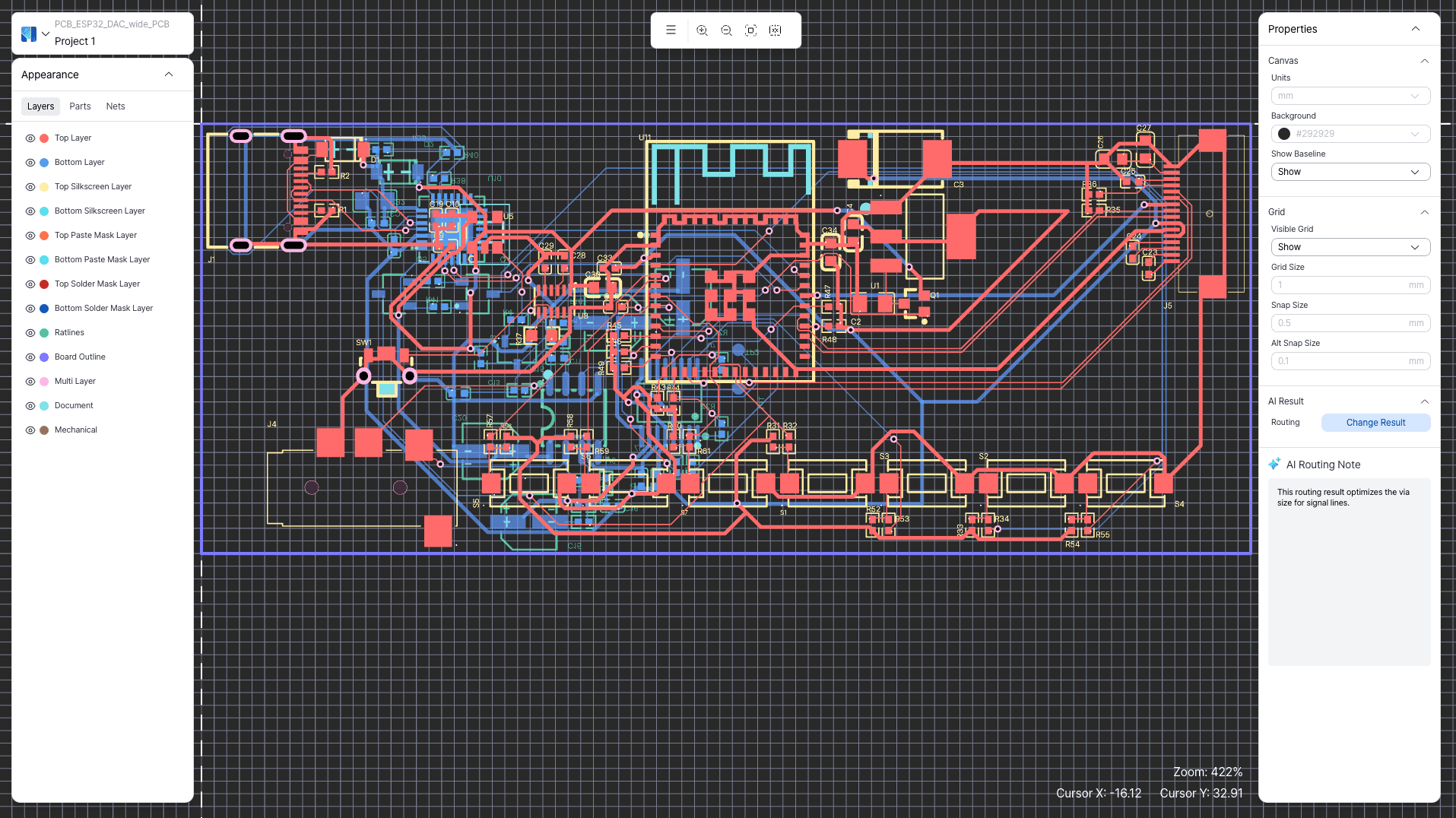
Offload the hurdles of complex multi-layer placement and routing to the AI EDA platform, MODI Factory, and focus on bringing your core design logic to life.
✅ Recommended for:
Junior engineers and university students struggling to determine the optimal layer count for their capstone projects or first industry designs.
Hardware designers looking for clear, logical criteria to balance manufacturing costs (2-layer) against circuit stability (4-layer).
Anyone tackling their first 4+ layer PCB design and feeling overwhelmed by complex via transitions and tangled routing.
Junior engineers and engineering students designing PCBs always face the same dilemma:
"Is a 2-layer board enough for this circuit, or should I go with 4 layers?”
Using too few layers can lead to tangled traces, excessive noise, and costly board re-spins. On the other hand, adding unnecessary layers raises prototyping and manufacturing expenses.
To help you find the sweet spot for your project, here is a practical guide to the characteristics of each PCB layer count and the key decision-making criteria used in real-world hardware design.
1. Understanding PCB layers in 60 seconds
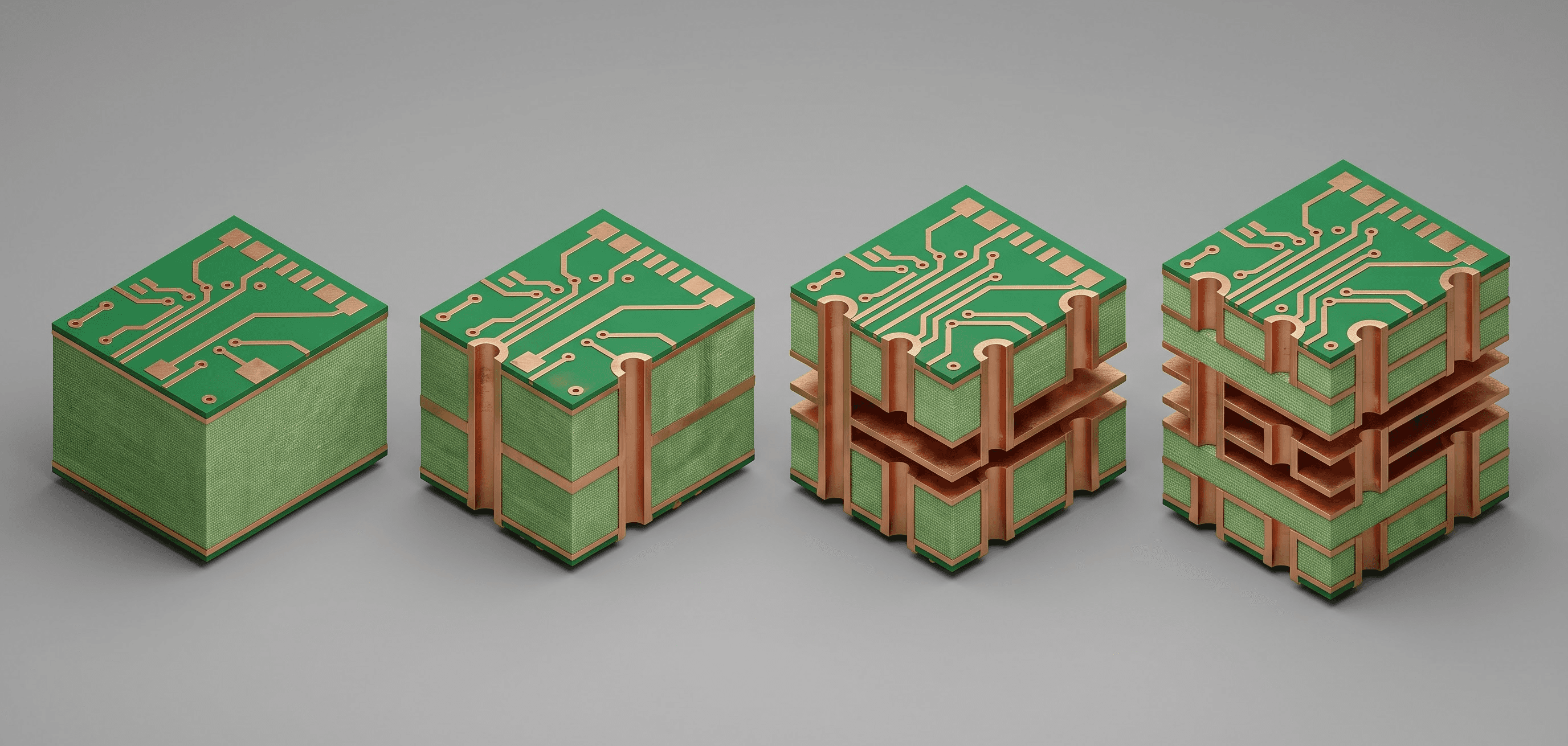
In PCB design, "layer count" does not simply refer to board thickness; it indicates the number of conductive copper layers carrying signals and power:
Single-layer (1-layer): Copper traces and components reside on only one side of the substrate.
Double-layer (2-layer): Copper traces are routed on both the top and bottom sides of the board.
Multi-layer (4+ layers): Multiple copper layers are sandwiched together, incorporating internal copper planes between dielectric substrates in addition to the outer layers.
As layer count increases, you not only gain significantly more routing real estate, but you also gain dedicated ground (GND) and power planes. This dramatically improves power distribution stability and mitigates electromagnetic interference (EMI).
2. Layer selection guide based on circuit complexity
Recommended layer count guidelines based on circuit scale and component requirements include:
Layer count | Recommended projects & applications | Characteristics & selection rationale |
|---|---|---|
Single-layer |
| Best suited for ultra-simple circuits with virtually no overlapping traces. Primarily used in ultra-high-volume production where driving unit cost to the absolute minimum is essential. |
Double-layer (2-Layer) |
| Both top and bottom layers can be used for trace routing and ground pours. It is the most cost-effective and common configuration for academic capstone designs and junior projects. |
4-Layer |
| Allows a standard 4-layer stack-up (Signal / GND / Power / Signal) for stable power delivery and superior noise shielding. If your design involves RF signals or high-speed digital lines, 4 layers is effectively the bare minimum. |
6-Layer or higher |
| Required when high-pin-count BGA packages create severe routing bottlenecks, or for high-performance boards demanding strict analog/digital isolation and hardware-level security. |
3. Common layer selection mistakes made by students and juniors
Insisting on 2 layers just to cut costs
Many beginners, concerned about manufacturing costs, attempt to cram all traces onto a 2-layer board. Some even avoid adding ground copper pours out of a mistaken belief that using more copper drives up fabrication fees.
However, if your project involves Wi-Fi, high-speed USB, PMIC power circuits, or dense component placement rather than simple sensor logic, stubbornly sticking to 2 layers will backfire. Excessive noise and signal integrity issues will lead to erratic IC behavior, ultimately forcing schematic modifications and costly board re-spins (re-fabrication after design modification)—wasting far more time and money in the end.
With modern rapid prototyping services like JLCPCB and PCBWay, the price gap between 2-layer and 4-layer prototyping has narrowed substantially. When routing complex or noise-sensitive signals, choosing a 4-layer board from the start is the fastest route to reducing development cycles and avoiding fabrication failure.
3 hurdles juniors face when designing multi-layer PCBs
Even after deciding to move to 4 layers, junior engineers often hit practical roadblocks during layout:
Placement: Tearing up and redoing component placements repeatedly due to difficulties in visualizing signal flow across a 3D layer stack-up.
Routing: Wasting countless hours manually untangling crossed traces and managing excessive interlayer via transitions.
Verification: A lack of objective feedback or senior guidance to validate whether routing a critical signal on a given layer will introduce fatal noise or EMI issues.
4. Lowering the barrier to multi-layer PCB design with MODI Factory