Insights
・
.
.
Essential check before placing a PCB order: top 3 easily missed footprint mistakes
Even if your schematic is flawless, missing a footprint error could force you to scrap your hard-earned PCB entirely.
💡 At a glance
Schematic reviews only verify electrical connectivity and do not guarantee the physical dimensions or pin assignments of actual components.
Pin mapping reversal, pad size mismatch, and component clearance issues are common footprint traps for beginner engineers and students.
Utilizing an AI PCB design tool automates placement and routing while providing design rationale, drastically reducing the risk of a re-spin (re-fabrication after design modification) simply by uploading a schematic.
✅ Recommended for:
Undergraduate students preparing to order capstone design boards who worry, “Will it work on the first try?”
Graduate students who need to build custom test PCBs for lab research without a senior engineer or mentor to review their work.
Engineering students concerned about wasting limited budgets and missing deadlines due to re-spins caused by footprint mistakes.
1. The schematic looks fine, so why won't the board power on?
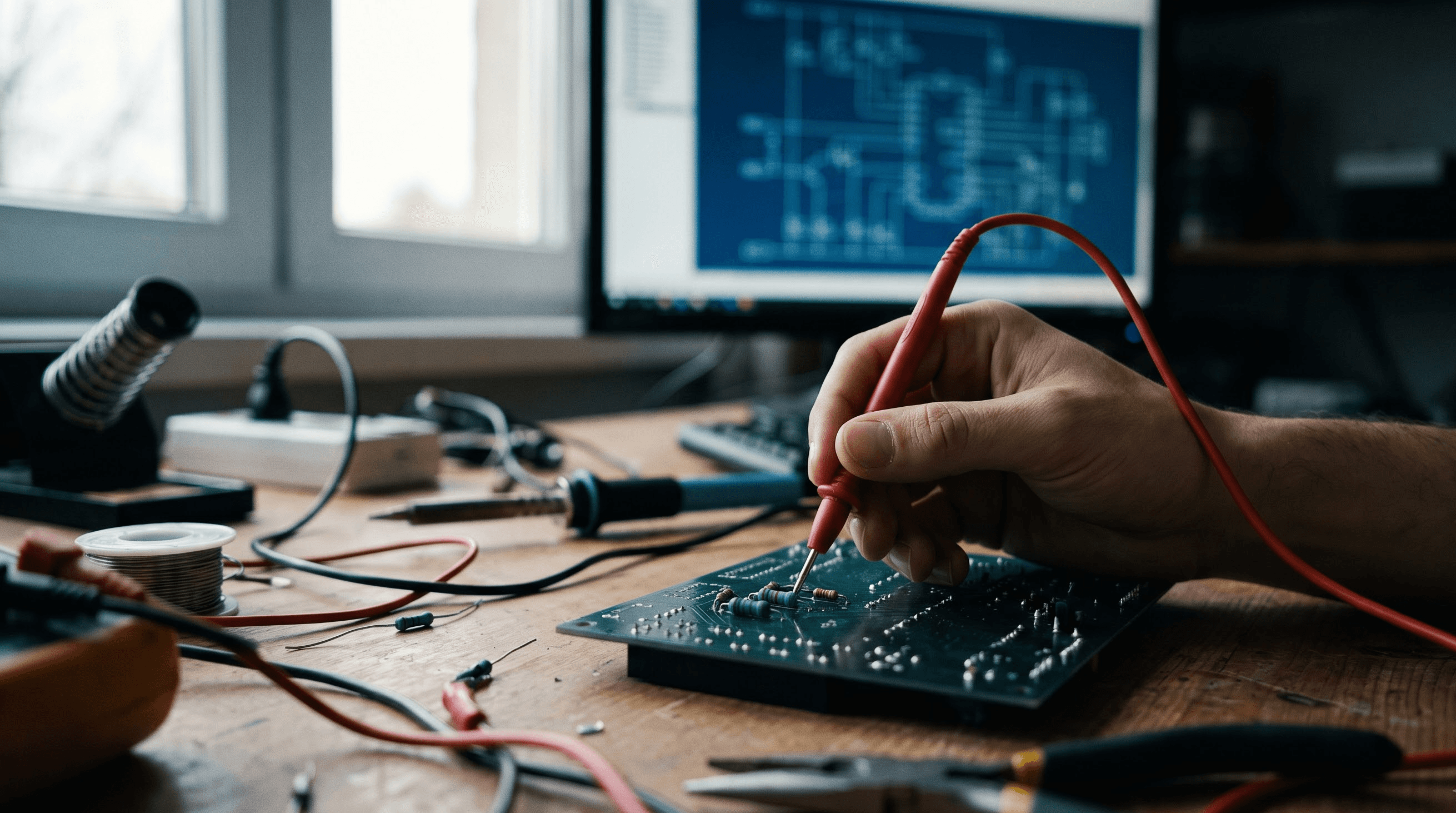
When building capstone projects or lab test boards, the most frustrating moment is applying power only to get zero response—or worse, a puff of smoke.
The core problem lies in the limitations of EDA tools. Even if you assign footprints to components in the schematic phase, ERC (Electrical rule check) only verifies logical pin connections between symbols. In other words, no automated check will verify whether the assigned footprint matches the physical dimensions or pinout of the real component.
Ultimately, even if a design passes schematic verification, any mismatch between physical components and footprint pads inevitably leads to assembly failure or power shorts.
2. Top 3 footprint mistakes beginner developers make
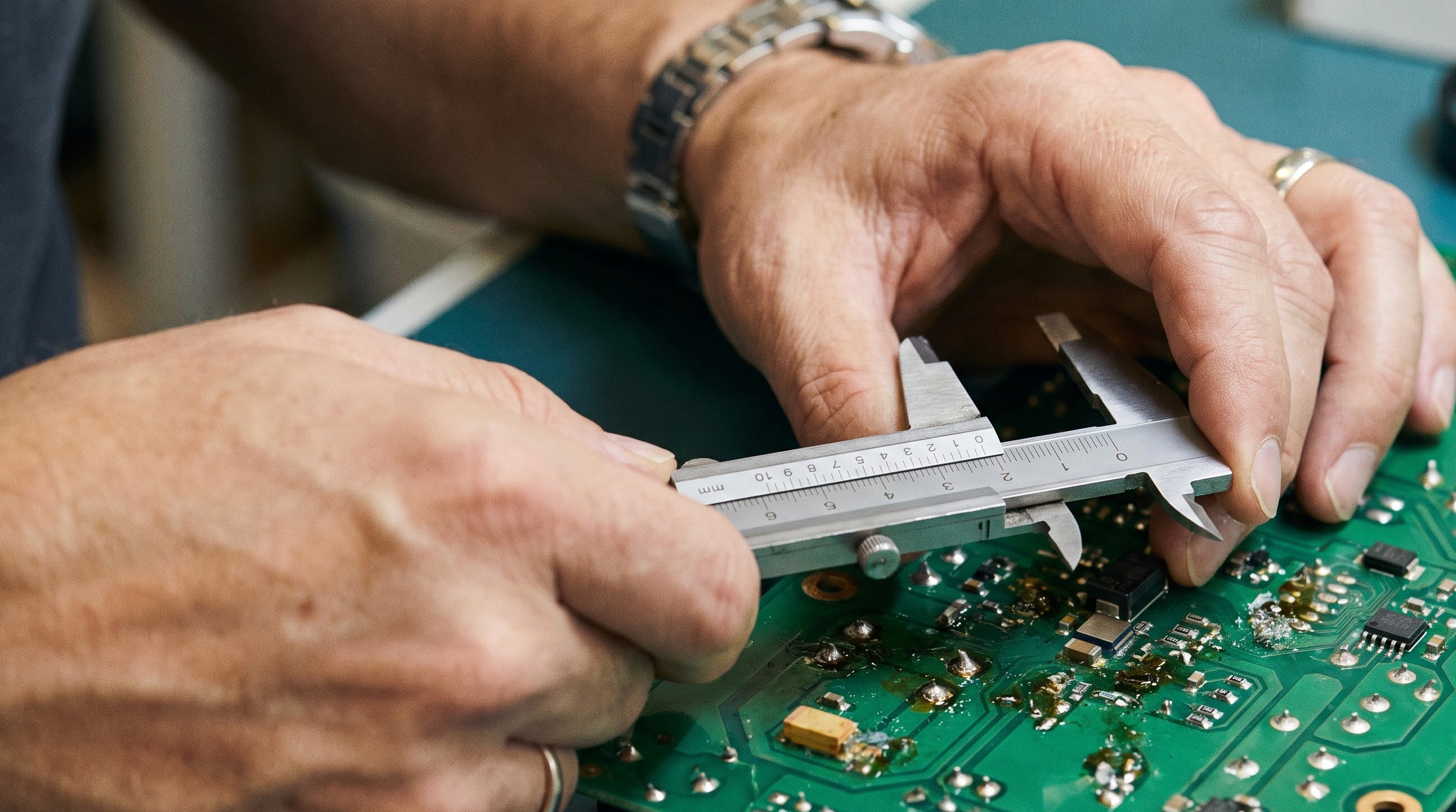
Pin mapping reversal caused by viewpoint confusion
Modern EDA tools automatically mirror pins when a component is placed on the bottom layer. Therefore, this mistake mainly occurs when creating a custom footprint or editing an existing library because the required footprint is unavailable.
If you misinterpret the viewpoint (top view / bottom view) of the pinout in the datasheet and apply a bottom view pinout directly to the top layer, the pin layout becomes horizontally mirrored when the physical component is mounted.
Common examples include packages like BGA (Ball Grid Array), LGA, and board-to-board connectors. BGA packages, in particular, often represent the ball layout from a bottom view (ball side view) in datasheets. If you mistakenly build a footprint assuming a top view, the pin assignment becomes completely inverted upon mounting on the PCB.
As a result, VCC and GND pins flip, instantly destroying the component upon powering on, or critical signal lines cross over, leading to catastrophic failure where the entire board must be discarded. Because bottom view representations are frequent not only in BGA or LGA but also in specific connectors, optical modules, and RF modules, you must double-check the datasheet viewpoint when creating library components.
Pad size mismatch: same name, different size
Pad dimension mismatches happen when footprints are selected visually or based solely on component names. Common examples include confusing 2.54 mm and 2.00 mm pin headers or SOP (1.27 mm pitch) and SSOP (0.65 mm pitch). However, the most frequent and fatal trap is confusing imperial and metric designations.
Even if both are labeled "0402", an imperial 0402 is 1.0 × 0.5 mm, while a metric 0402 measures only 0.4 × 0.2 mm (equivalent to imperial 01005). The same applies to 0603. Imperial 0603 (1.6 × 0.8 mm) and metric 0603 (0.6 × 0.3 mm, equivalent to imperial 0201) share identical names, making them easy to confuse in BOMs or library selection. Importing a library based solely on the name results in a footprint whose pads do not fit the actual part.
Physical clearance issues overlooked in 2D routing
Focusing only on 2D routing often causes engineers to overlook the physical volume of components like electrolytic capacitors, heatsinks, and connectors. Even if pin positions match, placing components too closely makes mounting physically impossible or leaves no room for assembly tools.
To prevent physical interference, you must understand and apply the courtyard concept defined by the IPC-7351 standard—the minimum 2D boundary area that accounts for component dimensions and assembly tolerances.
For instance, components such as electrolytic capacitors or heatsinks are easily placed right next to adjacent parts based only on simple circular or rectangular 2D footprints. However, ignoring courtyard and clearance (the minimum safety distance required to prevent electrical shorts and physical collision) can lead to overlapping component outlines, making soldering or tweezers usage impossible.
Easily missed footprint mistakes top 3 summary
Mistake type | Primary cause | Prevention point |
|---|---|---|
Pin mapping reversal | Applying a bottom view pinout to the top layer when creating libraries | Cross-check datasheet view perspective (top/bottom) against library pinouts |
Pad size mismatch | Confusing imperial/metric units or landing pattern variations | Verify unit designations and review manufacturer datasheet recommended landing patterns |
Physical interference | Checking only 2D routing without considering 3D component envelope | Inspect 3D views and clearance rules for adjacent parts, connectors, and enclosures |
3. Why footprint mistakes are fatal for undergraduate and graduate students
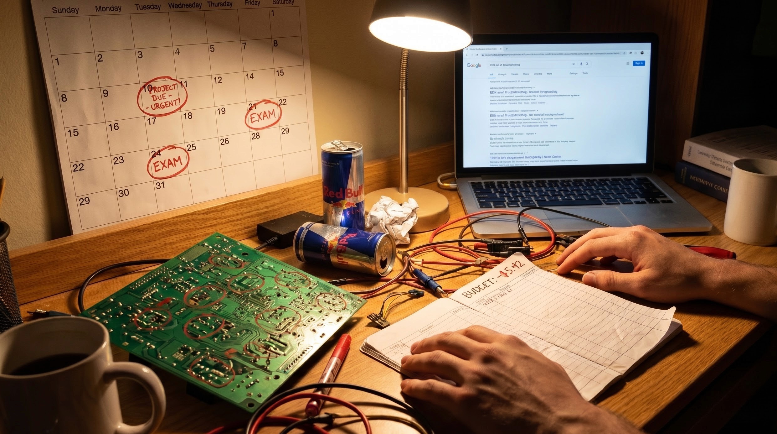
First, budgets are limited.
Student project budgets are tight. Even using low-volume overseas fabrication services costs tens of dollars, while domestic prototyping services, multi-layer boards, or rush orders can easily run into hundreds of dollars—a heavy financial burden for students. Adding the cost of repurchasing components damaged during desoldering and rework inflicts a severe hit on project funds.
Second, deadlines are tight.
With capstone presentations or assignment submissions approaching, low-volume PCB fabrication typically takes anywhere from several days to two weeks. If a footprint error requires a re-spin, over two weeks—including testing time—are wasted, making on-time submission nearly impossible.
Third, there is no senior engineer to review your work.
Unlike industry environments, academic settings rarely offer experienced senior engineers or mentors to thoroughly review your PCB artwork and footprints. Relying entirely on self-verification leaves students highly vulnerable to costly errors.
A footprint error does not merely waste material costs; it triggers a chain reaction of project delays. When final presentations or project deadlines are less than two weeks away, a single re-spin makes on-time submission virtually impossible.
4. Streamlining artwork completion after footprint setup: AI placement, routing, and design rationale