
Teams
・
.
.
Placing intent, not just coordinates
A conversation with Hugo, AI team — MODI Factory
Automated component placement. Three words that sound simple enough — until you realize that moving a single part by 1mm triggers a cascade of tradeoffs.
Every small decision carries a quiet question: Is this really the best I can do?
I wanted to know what it's like to live with that question every day.
So I sat down with Hugo, the engineer on MODI Factory's AI team who leads development of the auto-placement engine.
You'll want to read this if you're:
✅ Curious what PCB automation actually looks like in practice
✅ Interested in how engineers think when they've gone deep on a hard problem
✅ Wondering what it's like to work through a problem with no roadmap
✅ Want to understand the technical thinking behind how MODI Factory is built
Part 1. How MODI Factory began
Hugo, can you tell us what you do at MODI Factory?
I'm an algorithm developer on the AI team. My main focus is building the automated component placement engine.
You've been with MODI Factory since the early days. How does the original vision compare to what it is today?
The current product is focused on auto-placement and routing, but the original idea was much more ambitious. We wanted to build a one-stop platform that covered the entire PCB development process — from spec definition and component selection to schematic design, layout, and even procurement.
We also wanted to bring Luxrobo's MODI block-coding concept into circuit design. The idea was to turn schematics — which only specialists can read — into something like block diagrams that anyone could understand. So in the early stages, we were more focused on building a block-based component database, component search, supply chain integrations, and automatic schematic generation from user-created block diagrams.
But at some point it became clear that trying to cover the entire PCB workflow was too broad a scope. And in schematic design specifically, there were already strong competitors. So we made the decision to focus on auto-placement and routing. What you see today is the product of that pivot.
Part 2. From robotics major to circuit designer
Your academic background is a bit unusual. What drew you to robotics?
Demo video of a ROBOCUP entry robot with pose control applied (Source: Hugo)
I was always drawn to robots, and the robotics program offered something I really wanted: the ability to study both hardware and software — and actually build things. That combination was the biggest draw for me.
When I entered university, LLMs and GPT hadn't really taken off yet, so AI wasn't as accessible as it is now. It was a difficult domain to get into, but that's partly what made it compelling. There was real satisfaction in working through something hard.
I understand that around that time, your involvement with the robotics club Robit is what got you seriously interested in circuit design.
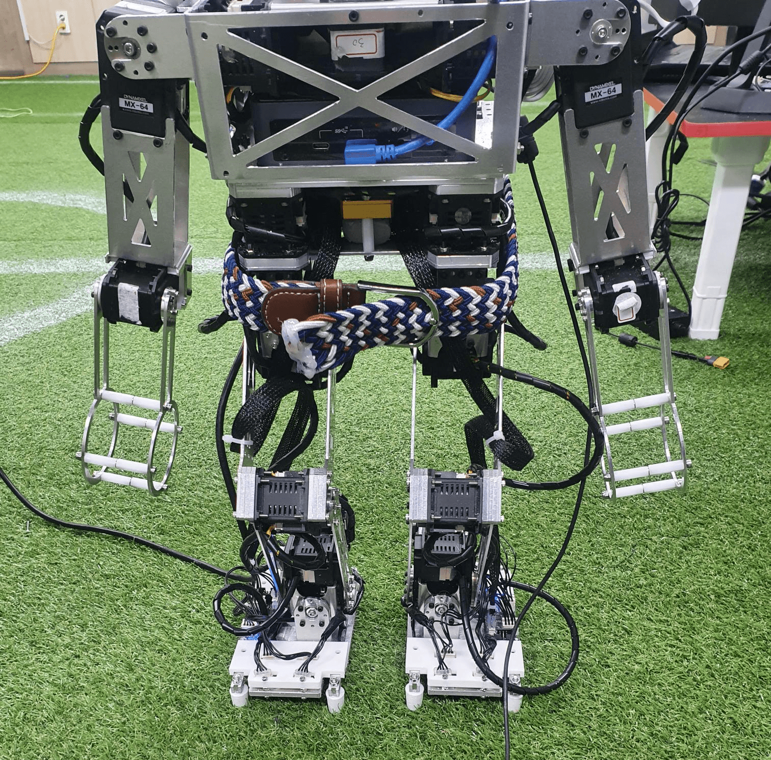
Close-up of the robot (Source: Hugo)
Robit is a competitive robotics team that participates in domestic and international tournaments. I worked on the humanoid division, where we built competition humanoids. One of my projects involved ZMP control — attaching force sensors to the feet, calculating the center of mass, and using that data to control the robot's walking posture. I designed the PCB and wrote the firmware myself. That's where my real interest in circuit design started.
Part 3. Component placement as urban planning
That hands-on PCB experience eventually led to the work you're doing now. How would you explain auto-placement to someone with no engineering background?
I think of PCB component placement like city planning — specifically like SimCity. At its core, it's the same problem: fitting things efficiently into a constrained space.
A city has residential zones, administrative zones, and commercial zones. A PCB has power component zones, analog zones, and MCU zones. Placement starts with defining those regions.
Just like every building needs roads and access points, every component needs space allocated for its routing. And just like you align buildings for urban aesthetics, you align components on a PCB — though there it's less about looks and more about manufacturability and assembly efficiency.
That's a useful way to think about it. When you first took on this problem, were there existing references you could build on?
Barely any. There was some research borrowing from semiconductor design methodology — VLSI — but nothing that performed at a usable level for our purposes.
So we started from scratch. We studied a wide range of real-world circuits and PCB designs, derived our own rules from what we observed, and built the initial engine around those rules.
Starting without any reference points — that must have been daunting. With so many constraints to juggle — electrical properties, heat, space, manufacturability — what was the hardest part?
The hardest part wasn't any single physical constraint. It was managing the tradeoffs between constraints — deciding what to give up in order to gain something else.
On a PCB, if even one connection fails, the board doesn't work. So the ultimate goal is always a placement where every net can be routed. But here's the counterintuitive part: a placement that looks inefficient on the surface is often the better choice once you factor in routing feasibility and surrounding context.
For example, pushing components closer together might shorten visible trace lengths — but it can also push decoupling caps away from their power pins, or force connectors that belong on the board edge to end up buried in the middle. The numbers look better; the actual placement is worse.
Finding the right rules, and deciding which objective to sacrifice when multiple goals conflict, was genuinely hard. Optimizing for a single metric is straightforward. Balancing routability, decoupling proximity, alignment, and edge placement simultaneously — and converging on something a human engineer would actually trust — that's a completely different class of problem.
Part 4. What MODI Factory does differently
After all that iteration, how would you describe what sets MODI Factory apart from other tools?
We benchmarked against commercial auto-placement tools and a general-purpose LLM baseline across four production boards, using the same scoring criteria. A few things stood out clearly.
The biggest difference is that MODI Factory places components based on what the product is for. The tools we compared against worked primarily around coordinates and cost functions. MODI Factory's engine takes a fundamentally different approach.
We split components into two categories. Components whose position depends on use context — MCUs, USB ports, buttons — are handled by an LLM that reads design intent. Passive support components like resistors and capacitors go through a quantitative evaluation loop. This is how the engine can actually interpret intent like "USB port should face outward" or "arrange 12 keypad switches in a 4×3 grid." MODI Factory was the only tool in the benchmark that satisfied design intent specs across all four boards.
The second difference is that we don't optimize for any single metric. We look at trace length, congestion, decoupling proximity, alignment, and edge placement together. One competing tool produced a result with 34% shorter trace lengths — which sounds impressive until you realize it got there by clustering all the pin headers next to the MCU. Decoupling coverage was 0%. It met zero design intent specs. Great number, unusable board.
The third difference is that the output is ready to use. The tools we tested left dozens of violations per board — overlapping components, parts outside the board boundary — all requiring manual cleanup. We treat violation-free output as a baseline requirement, not a bonus. All four test boards came out 100% placeable, and the engine ran 3 to 12 times faster — typically 3 to 12 minutes per board.
The bottom line: MODI Factory approaches placement as an understanding problem, not a coordinate optimization problem. That's the core difference.
What problems are you hoping to tackle next?
Hugo, MODI Factory AI Team

